Fundamentals of Signal Integrity
Summary
LeCroy Corporation, in association with Signal Consulting, Inc., has prepared an eight-part series on the fundamentals of signal integrity. Authored by the world’s foremost authority on signal integrity, Dr. Howard Johnson, the series is a “must read” for engineers who need a clear understanding of issues essential to high-speed performance.
Other papers in the series include Confirm The Diagnosis, Adequate Bandwidth, and Step Response Test. To read other parts in the series, please visit: http://www.lecroy.com
If you are just learning to make jitter measurements, begin with a calibrated source of jittery data. As you develop your measurement procedure, the calibrated source makes it easy to see, and easy to understand, what the many adjustments on your jitter-measuring equipment actually do.
Jitter Creation
The circuit in Figure 1 creates a wonderfully jittery clock. The clock source is a low-noise RF oscillator. The RF oscillator pumps out a 10-MHz sine wave at +12 dBm. On top of that sine wave I superimpose a phase-modulating signal.
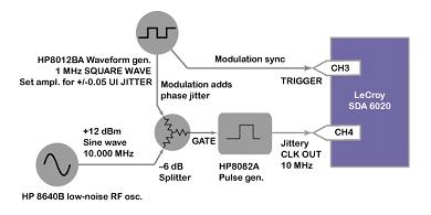
Figure 1 - Square wave modulation creates sudden shifts in the clock phase.
The superposition (adding) is accomplished with a passive device called a -6dB passive splitter. A three-port splitter is made from three 17-ohm resistors connected in a "Y" configuration. The only trick is getting it to work smoothly from DC all the way up through the GHz range. Figure 2 shows a typical 3-port splitter. The three ports are all interchangeable. In ordinary use, you apply an input signal to any one of the three ports. The splitter passes the signal through to both the other ports at half amplitude. For proper operation you must terminate each port (including the input) with a 50-ohm load.

Figure 2 - This three-port splitter comes equipped with SMA connectors. The port on the left has an SMA-BNC adapter added to it.
It turns out that any passive device that splits one input into two outputs can also be used backwards to combine two inputs into a single output. In my jitter-generation application I use the splitter in that mode to combine two signals. Provided that all three ports of the splitter lead to 50-ohm devices, the output of my splitter equals the sum of its two inputs, divided by two (the average of the inputs). The effective input impedance looking into each port of the splitter is 50 ohms. The gain from each input to the other outputs is one half, which is why it is called a -6 dB splitter.
Going back to Figure 1, the phase-modulating signal is a 1-MHz square wave. As the square wave goes up and down it changes the DC bias level of the sine wave carrier passing through the splitter. Changing the DC bias level affects the precise position of the sine wave zero crossings. Specifically, a positive bias equal to 30% of the sine wave amplitude advances all the rising edges by 5% of the cycle time and retards the falling edges by the same 5%. In that way the phase modulation changes the duty cycle of the clock output. The pulse generator that follows is used in GATE mode. It simply squares up the clock signal, producing a digital-looking waveform with edges located at the prescribed zero-crossings of the input signal.
I like this circuit because it's simple. By calibrating the amplitude of the phase-modulation signal compared to the RF carrier (both as measured at the output of the splitter), you can create precise amounts of phase modulation. When you choose your test equipment for this circuit, remember that the quality of the RF signal source directly affects the result. Any jitter present in the source translates directly to the output, plus any phase modulation you have added. Therefore, if you want accurate results, use a high-quality, low-noise RF source. The HP8640B I used is a rather old 20th-centruy device based on a very high-Q mechanically tuned resonator. The phase noise is extraordinarily low. Although you can get a digitally synthesized source today with slightly better performance, I don't think you can beat the price of an old used HP8640B.
Figure 3 shows the jittery CLK OUT signal produced with the following settings: Clock frequency=10 MHz, modulating frequency=1 MHz. The square wave amplitude equals 30% of the sine wave carrier amplitude. I've intentionally chosen a rather low clock frequency in this picture so you can see the individual clock transitions. At 100 MHz or higher the signal at this scale of time would just look like a blur.
In this circuit positive phase modulation enlarges the duty cycle of CLK_OUT, creating fat-topped cycles. Compared to an ideal clock at the same frequency, the rising edges in the fat-topped portion of the signal appear earlier than expected. Negative phase modulation reduces the duty cycle, creating a fat-bottomed signal with late rising edges.
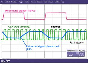
Figure 3 - The TIE@LEVEL measurement function acts as a phase detector.
The top waveform in the graph (pink) represents the modulating signal on a vertical scale of 100 mUI per division. The abbreviation "UI" means "unit interval". In this case one unit interval equals the clock period of 100 ns.
CLK_OUT is the fast-moving green signal in the middle on a vertical scale of 2 V per division.
The blue trace in the center of Figure 3 represents the phase of CLK_OUT, as detected by my LeCroy SDA6020 scope. The blue trace was computed using the scope's internal Time-Interval-Error (TIE) measurement function called TIE@LEVEL.
The TIE function displays jitter
The LeCroy SDA6020 scope provides a Time-Interval-Error (TIE) measurement function called TIE@level. I just call it the "TIE function".
You may think of the TIE function as a kind of "phase detector". It detects the incoming signal phase relative to an internally synthesized, ideal reference clock at the same frequency.
The TIE function is one of many built-in functions provided for the purpose of characterizing jitter.
The TIE function is a measurement function in the LeCroy SDA6020 (as opposed to a math function). The TIE function maps a vector of data samples to a vector of output points. The data samples must be captured together in one continuous real-time burst. Such a collection of data samples in called, in LeCroy terminology, a "trace". A trace may contain a large number of sampled data points.
The TIE function produces a vector of output points, each point corresponding to one edge in the input trace. There are usually far fewer points in the TIE output than in the TIE input trace, according to how aggressively you have over-sampled the input signal.
I have configured the TIE function to measure a clock signal (Figure 4). If you choose, "Input is: DATA", the function works on data signals as well.
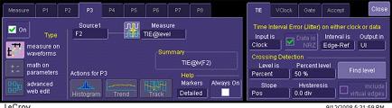
Figure 4 - The TIE function provides a multitude of options.
The setting: "Interval is: Edge-Ref" makes the TIE measure, at each signal edge, the degree to which that edge appears early or late compared to an internally synthesized, ideal reference clock at the same frequency. If you choose "Interval is: Edge-Edge" it just compares each signal edge against the next.
The TIE function lets you measure rising edges, falling edges, or both. If you select “Level is: Percent” it lets you choose the level (percentile of signal swing) at which the edge timing is measured, which explains the "@level" notation in the TIE@level measurement function name.
The adjustable threshold crossing level is provided so you can assess the degree of increase in jitter expected with variation in the input threshold of your receiver.
For clock analysis I choose rising edges only at the 50% level, with no hysteresis. For data analysis I choose both edges at the 50% level.
Displaying the result
Either the TREND function or the TRACK function can convert the TIE output into a data trace suitable for viewing or further processing. Both TREND and TRACK are math functions.
The difference between the two functions is the number of output points they create.
The TREND function outputs only the subsampled vector of reported results from TIE, leaving it up to you to figure out the horizontal scale (for clock analysis it would be one UI per point). The TREND function is useful when working with highly over-sampled data waveforms, because it reduces the number of data points to a manageable amount. Working with a 200MHz clock, for example, you might capture 10 million data samples representing 100,000 rising edges. The TREND function produces a vector of exactly 100,000 points.
The TREND function must be configured according to the number of points you wish to keep. In the context of jitter analysis, ensure that the number of points you ask for is less than the number of edges you are guaranteed to receive during one coherent blast of data sampling. Otherwise, the TREND function will attempt to collect the required number of data points from two or more successive data captures, thus intermixing data from non-coherently sampled sequences.
The TRACK function interpolates between the sub-sampled input points, producing a full-resolution trace with the same number of points as the original source waveform so there is no doubt about the horizontal scale. There is no more information contained in a TRACK display than a TREND display, it's just a choice of whether to interpolate the output, and how to interpret the horizontal scale. The disadvantage to TRACK is that, for my example with 10 million data samples, you get 10 million output points. If you are planning some FFT processing of the TIE track, that can be too many.
Figure 2 displays TIE information using the TRACK function. The vertical scale of the TIE trace is 100 mUI/div. The horizontal scale equals 200 ns/div. The CLK_OUT and TIE traces were generated together from one continuous sweep of 5000 points taken at 1 GS/s.
Because the TIE@LEVEL function reports new phase information only once after each signal edge, the TIE output appears highly sampled in time. The scope display linearly interpolates between reported values. Each time the modulating signal changes state, it takes at least one and sometimes two clock cycles for the detected phase to fully respond. Two clock cycles might be needed if, for example, the modulating signal changed state right on top of a sine wave zero crossing, producing this sequence of phase numbers: –.05, 0, and +.05 UI.
The TIE@LEVEL track appears antipodal to the modulating signal for purely semantic reasons. My modulating signal, when high, advances rising edges of the clock. An advance in time, compared to the ideal internal reference clock presents itself in the TIE track as a negative signal.
The TIE function provides several choices for synthesizing its internal reference clock. This article contemplates only one method, the simplest one, called "PLL_OFF", which is accessed under the TIE "VCLOCK" information tab.
Given an input trace, the PLL_OFF method constructs one continuous, single-frequency timing reference spanning the entire captured data record. You may imagine that it divines the correct frequency by simply counting the number of edges observed in the allotted time of one sample trace.
The process of finding the correct frequency is activated by the "FIND FREQUENCY" button under the "VCLOCK" tab of the TIE configuration screen. Given the correct assumed frequency, the TIE function then creates a comb of perfect clock edges at that frequency. Finally, it slides the comb back and forth until it achieves the best alignment with the incoming signal. The algorithmic details are considerably more complex, but this simplified conceptual explanation will suffice.
How the TIE function measures incoming signal phase
Once the comb has settled, the TIE@LEVEL measurement function then makes up a list, edge by edge, of the differences between each incoming signal edge and its corresponding "ideal" position. The TIE function can, if requested, track phase differences in excess of one unit interval (one clock period). It can also, if asked, measure phase differences between incoming data edges, both rising and falling, as opposed to just rising edges as I have configured it for this example.
Because the TIE@LEVEL internal reference is derived from the data itself, the TIE output is somewhat self-referential. What the TIE function actually reports, when you really think about it, is the local deviation in phase compared to the average phase established by the surrounding data record.
If the average phase of the surrounding data record does not properly represent the true average phase of the complete real-time input signal, then the TIE function cannot do its job. In practical terms this means that:
You must capture a suitably long input data record in order for the TIE function to work properly.
The problem of deciding how much data to capture, in order that the TIE function be able to synthesize a truly representative internal reference clock, is one of a general class of problems in the field of statistics that I shall discuss in my next article.
Best Regards,
Dr. Howard Johnson
*博客内容为网友个人发布,仅代表博主个人观点,如有侵权请联系工作人员删除。